


Materials with a special kind of boundary between crystal grains can deform in unexpected ways. Researchers have discovered an unexpected property of some nanostructured metals, could lead to new ways of 'tuning' their properties.
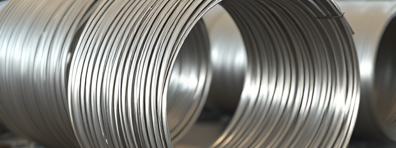
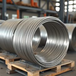
The experiment was carried out with copper, but the results should apply to some other metals with similar crystal structures, such as gold, silver, and platinum. These materials are widely used in electronic devices, Dao says. "If you design these materials" with structures in the size range explored in this work, which involves features smaller than a few hundred nanometers across, "you need to be aware of these kinds of deformation modes."
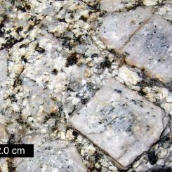
The sliding of a perfect twin boundary, with mirrored crystal lattices on both sides, was long considered to be impossible at room temperature in metals.
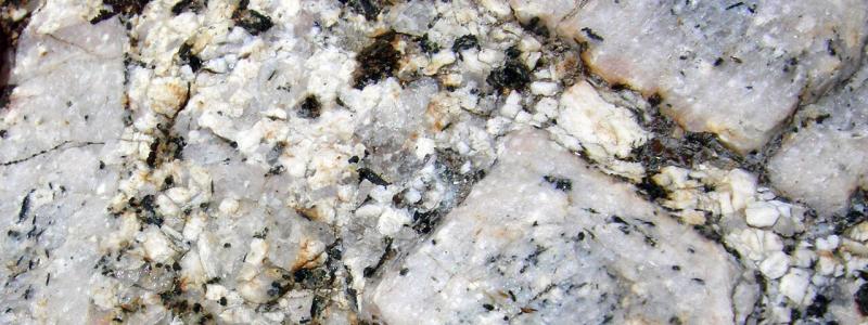
Most metals and semiconductors, from the steel in a knife blade to the silicon in a solar panel, are made up of many tiny crystalline grains. The way these grains meet at their edges can have a major impact on the solid's properties, including mechanical strength, electrical conductivity, thermal properties, flexibility, and so on.
When the boundaries between the grains are of a particular type, called a coherent twin boundary (CTB), this adds useful properties to certain materials, especially at the nanoscale. It increases their strength, making the material much stronger while preserving its ability to be deformed, unlike most other processes that add strength. Now, researchers have discovered a new deformation mechanism of these twin crystal boundaries, which could help engineers figure out how to more precisely use CTBs to tune the properties of some materials.
Contrary to expectations, it turns out that a material's crystal grains can sometimes slide along these CTBs. The new finding is described in a paper published this week in the journal Nature Communications by Ming Dao, a principal research scientist in MIT's Department of Materials Science and Engineering; Subra Suresh, the Vannevar Bush Professor Emeritus of Engineering and president-designate of Nanyang Technological University in Singapore; Ju Li, the Battelle Energy Alliance Professor in MIT's Department of Nuclear Science and Engineering; and seven others at MIT and elsewhere.
While each crystal grain is made up of an orderly three-dimensional array of atoms in a lattice structure, CTBs are places where, on the two sides of a boundary, the lattice forms a mirror-image of the structure on the other side. Every atom on either side of the coherent twin boundary is exactly matched by an atom in a mirror-symmetrical location on the other side.
Much research in recent years has shown that lattices that incorporate nanoscale CTBs can have much greater strength than the same material with random grain boundaries, without losing another useful property called ductility, which describes a material's ability to be stretched.
Some previous research suggested that these twin crystal boundaries are incapable of sliding due to the limited number of defects. Indeed, no experimental observations of such sliding have been reported before at room temperature. Now, a combination of theoretical analysis and experimental work reported in the Nature Communications paper has shown that in fact, under certain kinds of loads these grains can slide along the boundary. Understanding this property will be important for developing ways to engineer material properties to optimize them for specific applications, Dao says.
"A lot of high-strength nanocrystalline materials [with grains sizes measured in less than 100 nanometers] have low ductility and fatigue properties, and failure grows quite quickly with little stretching," he says. Conversely, in the metals that incorporate CTBs, that "enhances the strength and preserves the good ductility."
But understanding how these materials behave when subjected to various mechanical stresses is important in order to be able to harness them for structural uses. For one thing, it means that the way the material deforms is quite uneven: Distortions in the direction of the planes of the CTBs can happen much more readily than in other directions.
Source: MIT


